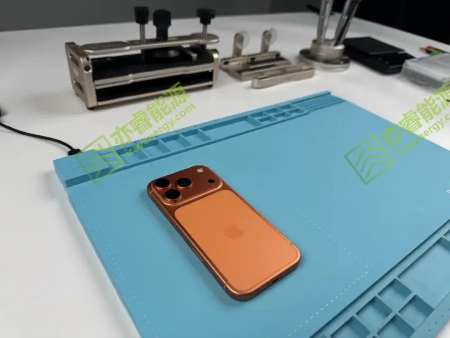
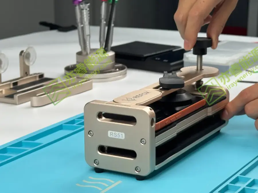
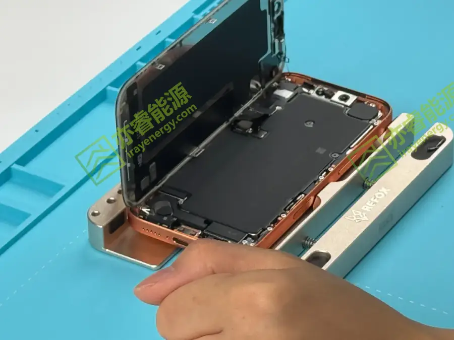
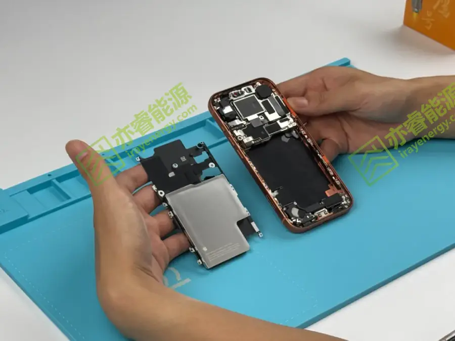
Teardown of the iPhone 17: A Close Look at Apple’s Top-Tier Hardware Design!

Tel: +8615017914702 | Whatsapp/Skype: +8615017914702 | Email: allen@irayenergy.com
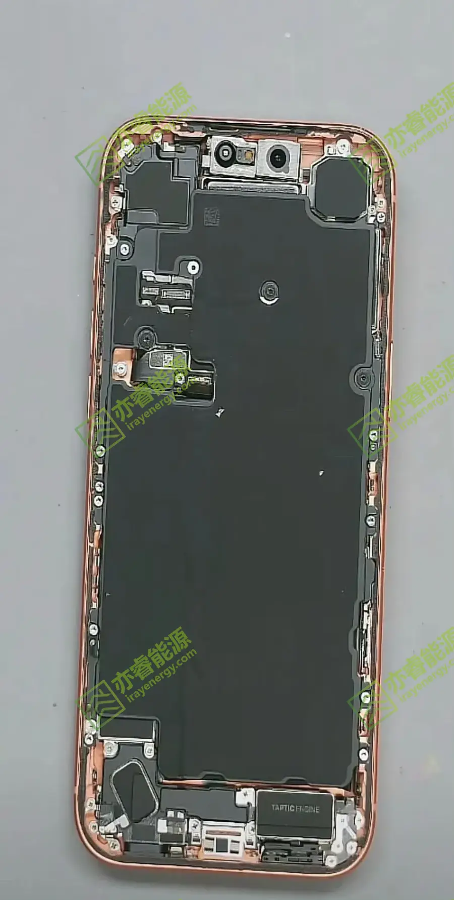
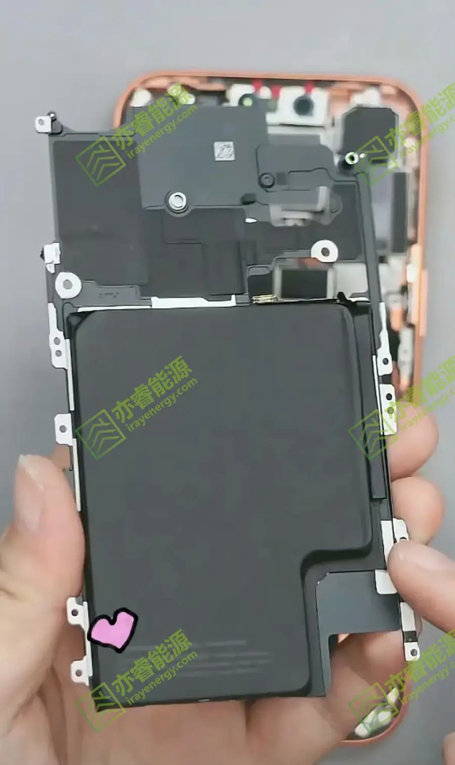
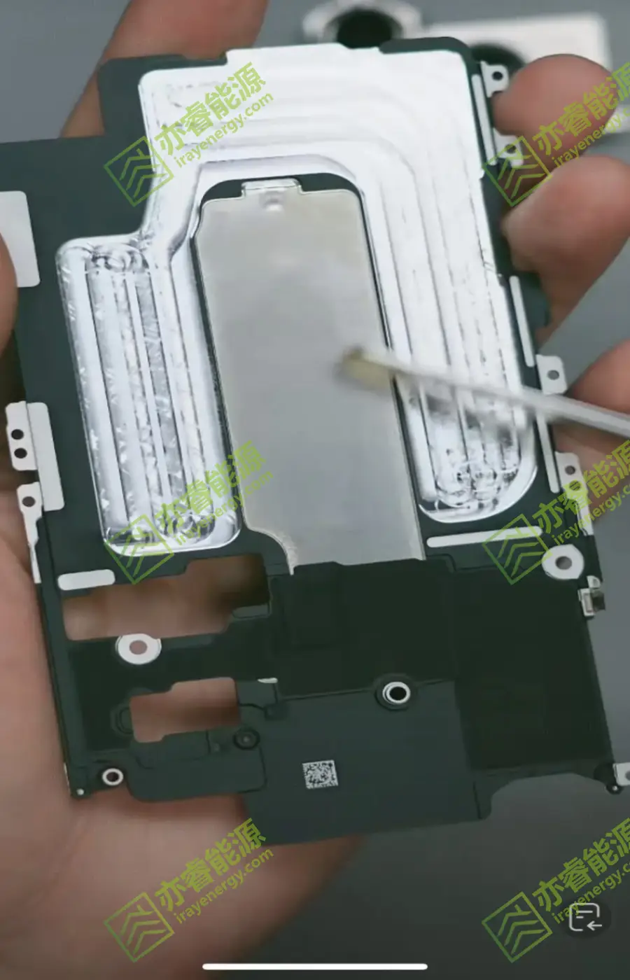
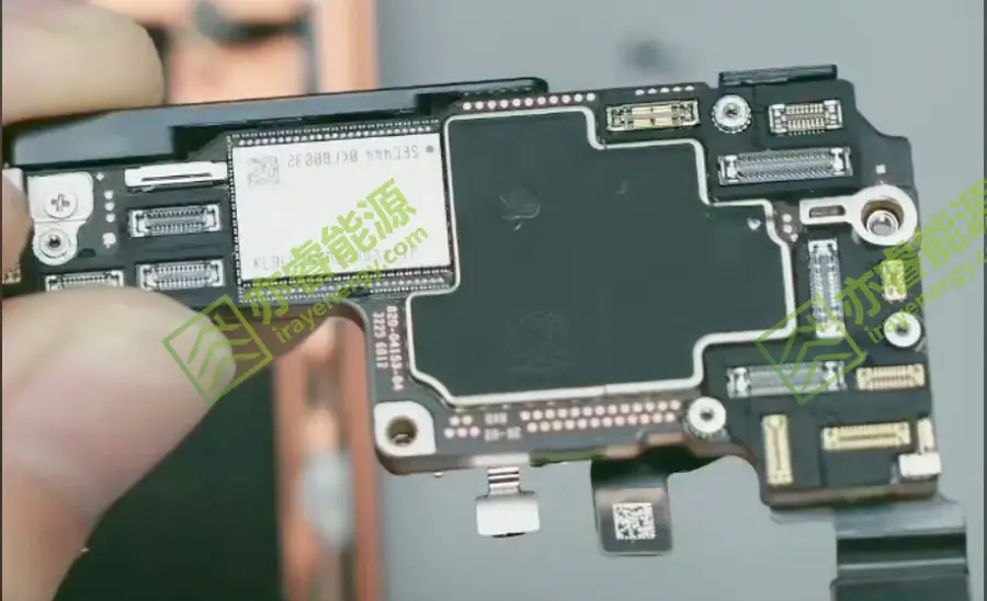
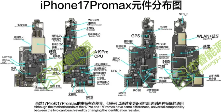
In the world of smartphones, Apple has always been renowned for its exceptional industrial design and precise internal architecture. Each generation of the iPhone represents a perfect fusion of technology and aesthetics. The brand-new iPhone 17 further exemplifies Apple’s relentless pursuit of excellence in structural design, component stacking, thermal management, and energy efficiency.
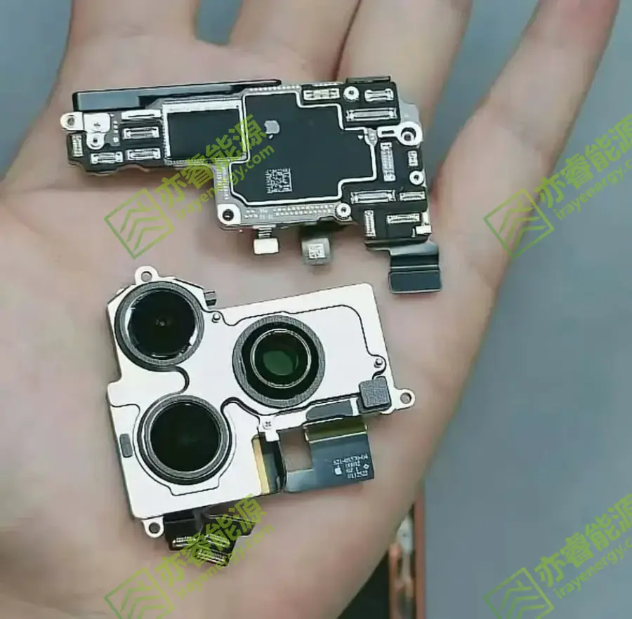
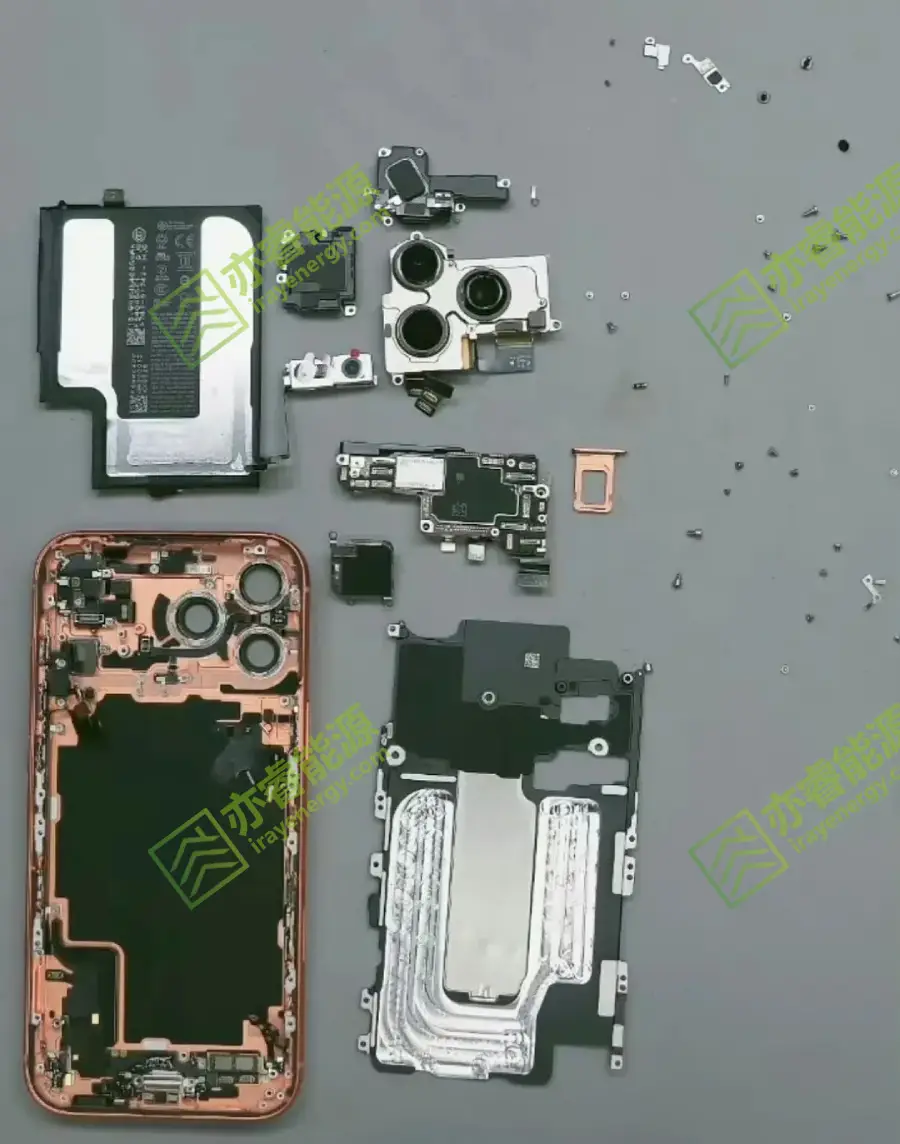
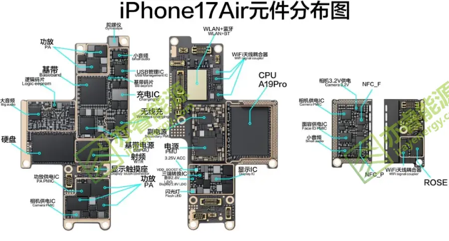
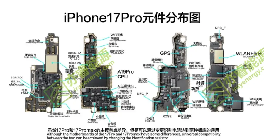
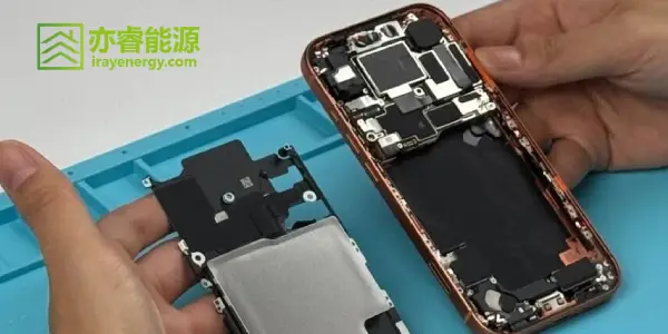
In this teardown, the IRAY Energy team will take you deep inside this flagship device to unveil the engineering beauty hidden beneath its elegant exterior. We’ll explore the motherboard layout, battery structure, camera module, and thermal system—analyzing how Apple achieves an extraordinary balance between performance and efficiency within such a compact form factor. Behind every screw, every flex cable, and every shielding layer lies Apple’s obsession with detail and its spirit of innovation.
Through this teardown, we can not only gain a direct understanding of the iPhone 17’s powerful hardware, but also appreciate Apple’s profound expertise and unique philosophy in electronic engineering design. This is more than just the disassembly of a smartphone — it’s a masterclass in industrial design and system integration.

If one were to look through the periodic table for a metal that is “naturally suited” for batteries, lithium would almost certainly rank first. It is the lightest metal element found in nature and possesses an extremely low standard electrode potential (–3.045 V vs. SHE). The combination of these two properties gives lithium an exceptionally…
With the global energy transition and low-carbon transformation accelerating, competition in electrochemical energy technologies has become a focal point. Lithium-ion batteries, backed by a mature industrial chain, are already widely used in consumer electronics and electric vehicles. Fuel cells, on the other hand, are highly regarded for their advantages in energy density and fast refueling….
In the field of battery R&D, the process is filled with the art of opposition and balance. Just as yin and yang coexist and depend on each other in nature, numerous parameters within a battery system often stand in opposition and mutual constraint. Energy and safety, capacity and lifespan, efficiency and yield — these conflicting…
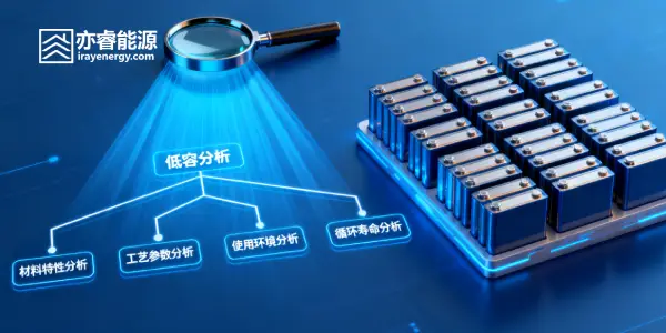
Capacity is one of the most critical performance indicators of lithium-ion batteries. Whether during sample validation or mass production, low capacity is one of the most troublesome problems. However, the causes of low capacity are often not singular—it usually results from a combination of factors involving design, material selection, process, operation, and testing.This article introduces…

I. Proposal of the Lithium-Ion Battery Concept and Early Exploration In modern battery technology, the lithium-ion battery is widely regarded as a truly revolutionary invention. The choice of lithium as the core element of this battery system is primarily attributed to its unique physical and chemical properties. Lithium is the lightest metal found in nature…
In lithium-ion battery R&D and manufacturing, people tend to focus their attention on the design parameters themselves—such as areal density, thickness, baking time, and so on.However, any process intended for mass production must include one crucial factor that is often overlooked: tolerance. Tolerance may seem insignificant, but it is the most important criterion for determining…
+8615017914702
+8615017914702
allen@irayenergy.com